Sharp CD-C482 Manuale di Servizio
Navigare online o scaricare Manuale di Servizio per Lettori CD Sharp CD-C482. Sharp CD-C482 Service manual Manuale Utente
- Pagina / 67
- Indice
- SEGNALIBRI
- CD-PC672 1
- SPECIFICATIONS 3
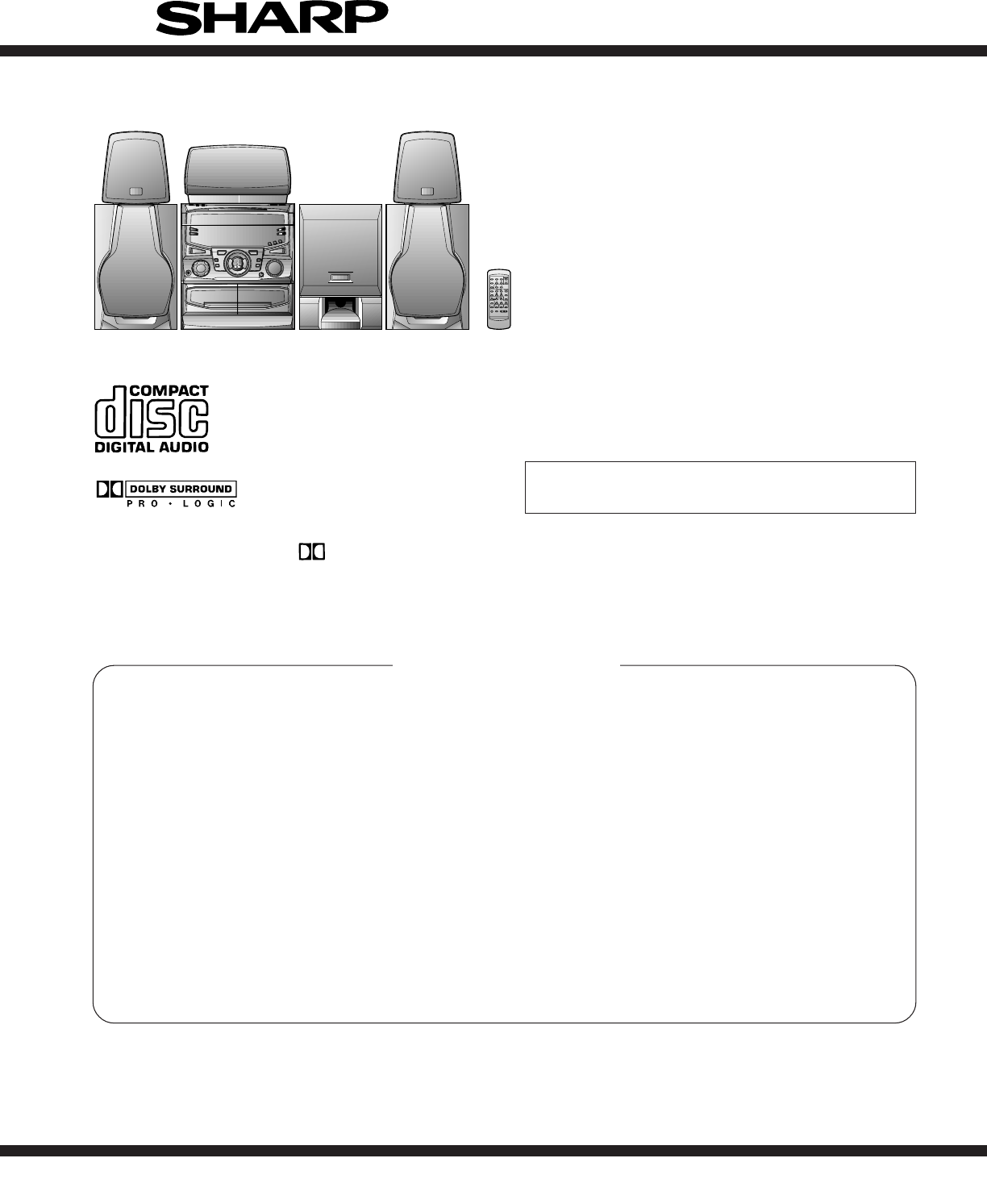
- NAMES OF PARTS 4
- ■ Rear panel 5
- ■ Front speakers 5
- ■ Centre speaker 5
- ■ Rear speaker 5
- ■ Sub woofer 5
- ■ Remote control 6
- ● Tuner control section 6
- ● CD control section 6
- ● Tape control section 6
- OPERATION MANUAL 7
- MINI COMPONENT SYSTEM 8
- Quick Guide/Guía rápida 8
- ADJUSTMENT 12
- NOTES ON SCHEMATIC DIAGRAM 13
- 8 9 10 11 12 20
- MAIN PWB-A1(2/3) 21
- FM SIGNAL 23
- AM SIGNAL 23
- MAIN PWB-A1 29
- SWITCH PWB-A3 31
- DISPLAY PWB-A2 31
- POWER PWB-C1 33
- WAVEFORMS OF CD CIRCUIT 38
- When the CD does not function 39
- Cleaning Disc 39
- PARTS CODE: 39
- UDSKA0004AFZZ 39
- Cleaner Liquid 39
- FUNCTION TABLE OF IC 44
- ANODE CONNECTION 51
- PARTS GUIDE 52
- RED BLACK 65
Sommario
– 1 –CD-PC672No. S4915CDPC672/ CONTENTSPageIMPORTANT SERVICE NOTES (For U.S.A. Only) ...
CD-PC672– 10 –Figure 10-1Figure 10-2Figure 10-3Be careful when installing the CD changer mechanism.Install the CD changer mechanism on the CD player b
– 11 –CD-PC672CP-C6721 Front Speaker 1. Net... (A1) x1 11-12. Front Panel ... (A2) x13. Screw ... (A
CD-PC672– 12 –MECHANISM SECTION• Driving Force CheckTorque MeterSpecified ValuePlay: TW-2412 Tape 1: Over 80 gTape 2: Over 80 g• Torque CheckTorque Me
CD-PC672– 16 –• The indicated voltage in each section is the one measuredby Digital Multimeter between such a section and the chas-sis with no signal
– 17 –CD-PC672 Figure 17 BLOCK DIAGRAM (1/3)27123418671824402045152316 262772252029212235143839284142 37 36PU-IN SWXL1XINLD0FIN2JP–CV+SLCSL1FIN1EFTOFD
CD-PC672– 18 – Figure 18 BLOCK DIAGRAM (2/3)IC9LA4POX501VOLUMEJOBVR7025 6 21162213201621171 3 242315201 22159 10117 113 4 5 6 10GND AM IF FM DET FM
– 19 –CD-PC672 Figure 19 BLOCK DIAGRAM (3/3)Q704IC951LA4551POWER AMP.IC803IC806IC805IC804IC650IC651Q601,Q602Q603, Q604KIA4558POPE AMP.IC601NJM4560DOPE
CD-PC672– 20 –Figure 20 SCHEMATIC DIAGRAM (1/12)ABCDEFGH123456• NOTES ON SCHEMATIC DIAGRAM can be found on page 16.D11SS133C77100/16R36220KC570.001R12
– 21 –CD-PC672Figure 21 SCHEMATIC DIAGRAM (2/12)78 9 10 11 12• The numbers 1 to 12 are waveform numbers shown in page 41.R54330R842.2KIC2LC78622
CD-PC672– 22 –ABCDEFGH123456• NOTES ON SCHEMATIC DIAGRAM can be found on page 16.Figure 22 SCHEMATIC DIAGRAM (3/12)R521 1KR522 1KC563 0.022 C532
CD-PC672– 2 –FOR A COMPLETE DESCRIPTION OF THE OPERATION OF THIS UNIT, PLEASE REFERTO THE OPERATION MANUAL.IMPORTANT SERVICE NOTES (For U.S.A. Only)BE
– 23 –CD-PC672Figure 23 SCHEMATIC DIAGRAM (4/12)78 9 10 11 12C62722/25 R449470 R450470 R62522R613100KR445330 C4420.001 R614 100KC60747/25 C609100PR6
CD-PC672– 24 –Figure 24 SCHEMATIC DIAGRAM (5/12)ABCDEFGH123456• NOTES ON SCHEMATIC DIAGRAM can be found on page 16.0V0V0V0.7V0V0V0V0.7V0V0V0.7V0V0.7V0
– 25 –CD-PC672Figure 25 SCHEMATIC DIAGRAM (6/12)78 9 10 11 12REC_MUTEA_12VBIASREC_RREC_LD_GNDTAPE_LM_GNDA_GNDTAPE_RT1/T20V0V0V0V0V11.6V 11.6V 11.7V 0V
CD-PC672– 26 –Figure 26 SCHEMATIC DIAGRAM (7/12)ABCDEFGH123456• NOTES ON SCHEMATIC DIAGRAM can be found on page 16.R32447C3160.022C3170.001C3328.2P(UJ
– 27 –CD-PC672Figure 27 SCHEMATIC DIAGRAM (8/12)78 9 10 11 12C3190.0047C3930.027(ML) C3560.022R35210KZD351DZ5.1BSB C35747/255C3541/50R3511.5KR386390CF
CD-PC672– 28 –ABCDEFGH123456• NOTES ON SCHEMATIC DIAGRAM can be found on page 16.Figure 28 SCHEMATIC DIAGRAM (9/12)R700 10K R719 10K R711 1KC
– 29 –CD-PC67278 9 10 11 12Figure 29 SCHEMATIC DIAGRAM (10/12)C710220/10C72210/50 C7230.1/50C7110.01D717DS1SS133L702100µH D715DS1SS133R78010K C7061/50
CD-PC672– 30 –ABCDEFGH123456Figure 30 SCHEMATIC DIAGRAM (11/12)R91122K R91022K R92122KR96139KIC901STK4084B POWER AMP. R8133.3(1/2W)C92547/50C91847/50
– 31 –CD-PC672Figure 31 SCHEMATIC DIAGRAM (12/12)78 9 10 11 1296139KQ906KRC107 MRL902 Q907KRC107 MR9644.7KR9654.7KC9370.047(ML) C9350.047(ML) C9400.
CD-PC672– 32 –Figure 32 WIRING SIDE OF P.W.BOARD (1/8)ABCDEFGH123456R614IC401 C305C320C304R316C314C308C312R301C311C324R322R323C310C306R315C351C352C350
– 3 –CD-PC672 Front speaker sectionType: 2-way 5-1/4" (13 cm) wooferand 2" (5 cm) tweeter typeMaximum input power: 80 WRated input power: 40
– 33 –CD-PC672Figure 33 WIRING SIDE OF P.W.BOARD (2/8)78 9 10 11 12IC501 R515R514R519R142R140R146C140R145R141R423C563R513C546R510R433R429R472R471C440C
CD-PC672– 34 –ABCDEFGH123456Figure 34 WIRING SIDE OF P.W.BOARD (3/8)IC70R782R783RD15RD16RD01R799RD10RD11R723RD06RD05C711RD03RD04R795R797C713C714RS701
– 35 –CD-PC672Figure 35 WIRING SIDE OF P.W.BOARD (4/8)78 9 10 11 12IC701 IC702 IC703 3 R742R743R744R760R759R758R751R763R764R762R765R766R767R768R778R77
CD-PC672– 36 –ABCDEFGH123456Figure 36 WIRING SIDE OF P.W.BOARD (5/8)D803D806D807D804D8057654321D809C813R806C825C803R933C801R932R969IC804D821CNP8067654
– 37 –CD-PC672Figure 37 WIRING SIDE OF P.W.BOARD (6/8)78 9 10 11 12SO901R96312345678910111213141516178R905C935D908R913C912R911C959C910IC803Q802D812D81
CD-PC672– 38 –Figure 38 WIRING SIDE OF P.W.BOARD (7/8)ABCDEFGH123456RCNPM1CNPM21212FWM1FWM2SWM3SWM4F. A. S(260-10)F. P. (260-9)1234567891011123421PHM1
– 39 –CD-PC672Figure 39 WIRING SIDE OF P.W.BOARD (8/8)78 9 10 11 12• The numbers 1 to 12 are waveform numbers shown in page 41.IC99L99C99C98BI99
CD-PC672– 40 –VOLTAGE0V-27.5V0V0V-27.5V-27.5V0V 0V0V-25.8V26.0V-0.15V987654321121110-0.1V-0.15V-24.6V -0.1V-0.1V-0.1V-27.5V0V1716151413201918PINNO.VOL
– 41 –CD-PC672WAVEFORMS OF CD CIRCUIT35ms0.50 VIC1 20 F.E15ms5.0 VIC1 54 DRFSTOP PLAYFOCUS SERCH1354267891011345678967810111296789120.5ms1.00 V
CD-PC672– 42 –TROUBLESHOOTING (CD SECTION)When the CD does not functionWhen the CD section does not operate when the objective lens of the optical pic
CD-PC672– 4 –NAMES OF PARTSCD-PC672 Front panel11. Disc Number Selector Buttons12. Disc Tray13. Multi Indicator 14. Disc Skip Button15. Open/Close Bu
– 43 –CD-PC672• When the turntable fails to stop.Is from 5 V till 2.5V down pulse (approx. 300 ms)Check the SWM3 and the wiring from the IC701 pin
CD-PC672– 44 –• When the CD tray fails to open or close.Is there following voltage input in specific state of IC701 pin 19? Open state: 0V Cl
– 45 –CD-PC672• Playback can only be performed when a disc isloaded.Is HF waveform normal (see the Fig.45-1, 2)?Check the tracking system. Is the Foc
CD-PC672– 46 –• Checking the spin system.YesNoPlay operation is performed without disc.The turntable rotates a little.The turntable fails to rotate o
– 47 –CD-PC672FUNCTION TABLE OF ICIC1 VHiLA9241M/-1: Servo Amp. (LA9241M) (1/2)1 FIN2 Connection pin for photodiode of pickup.RF signal is generated t
CD-PC672– 48 –IC1 VHiLA9241M/-1:Servo Amp.(LA9241M) (2/2)Pin No.Port NameFunction51 CL Micro computer command clock input pin.52 DAT Micro computer co
– 49 –CD-PC6721 DEFI Input Defect detection signal (DFF) input terminal. (When this terminal is not used, connect it to 0V.)2 TAI Input For PLL Input
CD-PC672– 50 –IC2 VHiLC78622N-1: Servo/Signal Control (LC78622NE) (2/2)47* SBSY Output Sub-code clock sync signal output terminal.48* EFLG Output C1,
– 51 –CD-PC6721 IN2- CH2 inverted input.2 IN1A- CH1 inverted input.3 IN1B- CH1 output offset control.4 OUT1- CH1 inverted output.5 OUT1+ CH1 non-inver
CD-PC672– 52 –IC701 RH-iX0301AWZZ:System Control Microcomputer (IX0301AW) (1/2)1 VDD VDD — (+) POWER SUPPLY2 P37 ENA Output DOLBY PROLOGIC ENABLE TER
– 5 –CD-PC672 Rear panel11.CD Digital Output Socket12.AC Power Lead13.FM/AM Loop Aerial Socket14.Video/Auxiliary (Audio Signal) Input Sockets15.Rear
– 53 –CD-PC672IC701 RH-iX0301AWZZ:System Control Microcomputer (IX0301AW) (2/2)56 P116 KEY JOG A Input KEY JOG INPUT A57 P115 KEY JOG B Input KEY JOG
CD-PC672– 54 –FL701 VVKBJ685GNK-1: FL DisplayFigure 54 FL DISPLAYS IC OS5S4S2S3DpS1B1 B2B3 B4 B5B6 B7B1B2B3B4B5B6B79G10G11G1G 2G 3G 4G 5G 6G 7G 8GB21B
– 55 –CD-PC672PARTS GUIDENOTE:Parts marked with “ ” are important for maintaining the safety of the set.Be sure to replace parts with specified ones f
PRICERANKDESCRIPTIONNO.PARTS CODENO. PARTS CODEPRICERANKDESCRIPTIONCD-PC672– 1 –INTEGRATED CIRCUITSIC1 VHILA9241M/-1 J AS Servo Amp.,LA9241MIC2 VHILC7
NO.PRICERANKDESCRIPTIONPARTS CODENO. PARTS CODEPRICERANKDESCRIPTIONCD-PC672C18 VCEAZA1HW474M J AB 0.47 µF,50V,ElectrolyticC19 VCEAZA1HW105M J AB 1 µF,
PRICERANKDESCRIPTIONNO.PARTS CODENO. PARTS CODEPRICERANKDESCRIPTIONCD-PC672C510,511 VCEAEA1HW474M J AB 0.47 µF,50V,ElectrolyticC512,513 VCEAEA1HW475M
NO.PRICERANKDESCRIPTIONPARTS CODENO. PARTS CODEPRICERANKDESCRIPTIONCD-PC672R40 VRS-TV2AB562J J AA 5.6 kohms,1/10WR41,42 VRS-TV2AB473J J AA 47 kohms,1/
PRICERANKDESCRIPTIONNO.PARTS CODENO. PARTS CODEPRICERANKDESCRIPTIONCD-PC672R620 VRD-ST2CD270J J AA 27 ohms,1/6WR621,622 VRD-MN2BD272J J AA 2.7 kohms,1
NO.PRICERANKDESCRIPTIONPARTS CODENO. PARTS CODEPRICERANKDESCRIPTIONCD-PC672CNP10 QCNCM705KAWZZ J AC Plug,10PinCNP11 QCNCM704FAWZZ J AC Plug,6PinCNP12
PRICERANKDESCRIPTIONNO.PARTS CODENO. PARTS CODEPRICERANKDESCRIPTIONCD-PC672209 MLEVP0067AWZZ J AC Lever,Lock210 LCHSZ0011AWZZ J AG Chassis,CD Mechanis
CD-PC672– 6 –CD-PC672 Remote control 11.Remote Control Transmitter LED12.Surround Level Buttons13.Centre Level Buttons14.Dolby Pro Logic Button15.Cen
NO.PRICERANKDESCRIPTIONPARTS CODENO. PARTS CODEPRICERANKDESCRIPTIONCD-PC672906 92L372-0106 J AB Screw,ø4×12mm907 92L372-0108 J AC Screw,ø3×10mm908 92L
CD-PC672– 64 –ABCDEFGH123456Figure 9 CD MECHANISM EXPLODED VIEW– 9 –CD-PC672306-1701304701302301702702303M1703x2703x2305x2SW4M2305PWB-D306-2306-33067
CD-PC672– 65 –Figure 10 CABINET EXPLODED VIEW (1/2)ABCDEFGH123456– 10 –CD-PC672247PWB-C2PWB-A1PWB-A2PWB-A4Silicongrease241-1245236606261x5207241-2202
CD-PC672– 66 –Figure 11 CABINET EXPLODED VIEW (2/2)ABCDEFGH123456– 11 –CD-PC672PWB-DCDMECHANISMPWB-B613229225228209224232604604229613225616x422921421
CD-PC672– 67 –ABCDEFGH123456Figure 12 SPEAKER EXPLODED VIEW (1/3)– 12 –CP-C672(withCapacitor C1,2)C1,2CapacitorTWEETERSP3(L-CH)SP4(R-CH)WOOFERSP1(L-CH
CD-PC672– 68 –– 13 –CP-SW672Figure 13 SPEAKER EXPLODED VIEW (2/3)ABCDEFGH123456RED BLACK901902SP1SP1905x4904906907903
CD-PC672– 69 –ABCDEFGH123456Figure 14 SPEAKER EXPLODED VIEW (3/3)– 14 –GBOXS0023AWM1901SP1,2SP1,2902904x6905903GBOXS0022AWM1904x4902904x4SP1901903905
CD-PC672– 70 –– 14 –PACKING OFF THE SET (For U.S.A. Only)Setting position of switches and knobsTape Mechanism STOP– 15 – Not Replacement ItemUNITSPAKP
– 7 –CD-PC672OPERATION MANUALSETTING THE CLOCK 1Press the POWER button to enter the stand-by mode.2Press the CLOCK button.3Within 5 seconds, press the
CD-PC672– 8 –MINI COMPONENT SYSTEMQuick Guide/Guía rápidaCD-PC672● Remote control x 1●Controlador remoto x 1● 2 “AA” batteries●Dos pilas “AA”Remote Se
– 9 –CD-PC672DISASSEMBLYCaution on DisassemblyFollow the below-mentioned notes when disassemblingthe unit and reassembling it, to keep it safe and ens
Più documenti per Lettori CD Sharp CD-C482

Prodotti e manuali riguardandi Lettori CD Sharp CD-C482
 (36 pagine)
(60 pagine)
(36 pagine)
(60 pagine)
 (57 pagine)
(40 pagine)
(57 pagine)
(40 pagine)


 (35 pagine)
 (12 pagine)
(40 pagine)
(28 pagine)
(12 pagine)
(40 pagine)
(28 pagine)
 (28 pagine)
(23 pagine)
(40 pagine)
(48 pagine)
(31 pagine)
(25 pagine)
(19 pagine)
(55 pagine)
(45 pagine)
(37 pagine)
(44 pagine)
(28 pagine)
(23 pagine)
(40 pagine)
(48 pagine)
(31 pagine)
(25 pagine)
(19 pagine)
(55 pagine)
(45 pagine)
(37 pagine)
(44 pagine)
© 2020, manymanuals.it. Tutti i diritti riservati | 0.106 s |
 Manymanuals.com
 Manymanuals.de
 Manymanuals.fr
 Manymanuals.it
 Manymanuals.pl
 Manymanuals.cz
 Manymanuals.es
 Manymanuals-pt.com
Commenti su questo manuale