Sharp ER-A440 Manuale Utente
Navigare online o scaricare Manuale Utente per Stampanti per fotografie Sharp ER-A440. Sharp ER-A440 User Manual Manuale Utente
- Pagina / 52
- Indice
- SEGNALIBRI
- SERVICE MANUAL 1
- CHAPTER 1. SPECIFICATIONS 2
- 3. Mode switch 3
- 4. Display 3
- 5. Printer (DP-730) 3
- 6. Drawer 4
- CHAPTER 2. OPTIONS 5
- 2. Options 6
- 3. Service options 6
- 4. Service tools 6
- 5. Supplies 6
- 6. Options 6
- CHAPTER 3. SRV. RESET AND 7
- MASTER RESET 7
- 1. Hard ware block diagram 8
- 2. Description of main LSI’s 9
- 2) Block diagram 10
- 3) Pin description 11
- 2-2. G.A (MPCA7) 12
- I/R Control 13
- 2-3. CKDC8 15
- 3. Clock generator 16
- 4. Reset (POFF) circuit 16
- 1) Memory map 17
- (OPTION) 18
- 1) Block diagram 19
- 2) SSP register 19
- 3) SSP register access method 20
- Relation ship among RP/HP/DP 21
- 7) Caution 22
- 1) Power on sequence 22
- 10. Power supply circuit 23
- (Not used) 24
- Key code 24
- 1 2 3 4 5 6 7 8 9 0 25
- 1 0 6 X-X 26
- 7-SEGMENT DISPLAY: 27
- [12] Standard ROM test 28
- [14] Option RAM test 28
- Normal end 29
- NGRS TEST ER XX 29
- RS TEST OK 29
- CHAPTER 6. DOWN LOAD 30
- FUNCTION 30
- (Baud rate setting: #903-A) 31
- 7. Operational method 32
- CHAPTER 7. SERVICE PRECAUTION 33
- POWER SUPPLY(MAIN PWB) 34
- 1. MAIN PWB CIRCUIT DIAGRAM 34
- CPU(HD6415108) 35
- GATE ARRAY(MPCA7) 36
- Not moun ted 37
- OPTION MEMORY (OPT CN) 39
- PRINTER & SENSER 40
- DISPLAY DRIVER(CKDC8) 41
- KEY I/F(MAIN PWB) 42
- 2. MAIN PWB LAYOUT 44
- (2) SIDE B 45
- 3. FRONT PWB/POP UP PWB 1/1 46
- 4. FRONT DISPLAY PWB 47
- 5. POP-UP PWB 1/1 48
- 6. POP-UP DISPLAY PWB 49
- 7. PS PWB 50
- 8. PS PWB 51
- SHARP CORPORATION 52
- Information Systems Group 52
Sommario
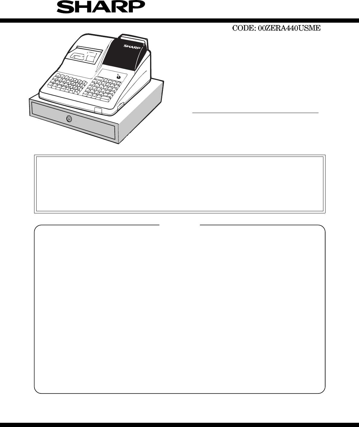
SERVICE MANUALELECTRONICCASH REGISTERMODEL ER-A440SRV Key : LKGIM7113RCZZPRINTER : DP-730("U" & "A" version)CAUTIONEXTREME CAU
2) Block diagramFig. 2-2P47FTI2P45FTI1P43P42P41/TMCIP40P37P36P35P34P33BREQBACKWAITP27/A23P26/A22P25/A21P24/A20P23/A19P22/A18P21/A17P20/A16A15A14A13A12
3) Pin descriptionPIN No.SYMBOLSIGNALNAMEIN/OUTFUNCTION1 INRESET INPUT from CKDC WUTHBUFFER2INNON-MASKABLE INTERRUPT INPUTFOR SSP INTERRUPT INPUT3 VSS
2-2. G.A (MPCA7)1) Pin configurationGATE ARRAY (LZ9AH39)MPCA7Fig. 2-31RF2JF3PCUT4FCUT5VF6STAMP7SLF8SLRS9SLMTD10RES11TRG12TRG13POFF14INT115HTS116SCK117
2) Block diagramFig. 2-4MTDMTDRJMTRSLMTDSLMTSSLMTRSLMTDTXDISCKIRXDIHTS1SCK1STH1HTS2SCK2STH2ROS1ROS2RAS1RAS2RAS3OPTCSASRDWRRDOWROΦRESETRESVRESCPOFFMD0M
3) Pin descriptionPinNo.SignalnameIn/OutFunction1 RF Out Receipt side paper feed solenoid2 JF Out Journal side paper feed solenoid3PCUT Out Printer pa
PinNo.SignalnameIn/OutFunction105 DAX2 — Nu106MCR1 — Nu107MCR2 — Nu108WAIT Out Wait request signal109EXWAIT In External wait control input signal110 R
PinNo.SYMBOLSIGNALNAMEIN/OUTFUNCTION33 KR7 KR7 IN KEY RETURN 734 AVRF GND35 AVDD VDD36 /RESET /RES0 IN37 XT232.768 KHz38 XT139 IC GND40 X24.19 MHz41 X
This circuit monitors +24V supply voltage.The voltage at the (–) pin of the comparator IC3A is always main-tained to 5.1V by means of the zener diode
RAM area memory mapFig. 5-4Note: RAS2 signal is formed as OR in the image area of 0 page.(lower32KB).I/O area memory mapFig. 5-5Note 1: MPCCS signal
6. SSP circuit1) Block diagramThis is the circuit employed to do the Special Service Preset(SSP). (Block diagram)Fig. 6-1(MPCA7 block diagram)Fig. 6-2
CHAPTER 1. SPECIFICATIONS1. Appearance/Rating1) RatingPower source AC 120 V ±10% 50/60HzPower consumption Standby: 11.5 WMaximum: 40 W (max.)Operating
3) SSP register access methodAccess to SSP break address register is performed through the tem-porary register as shown below:Fig. 6-5Enable flags can
<Motor lock protection>When an abnormal load is applied to the mechanism, the DP (DotPulse) frequency is checked to prevent against the motor bu
7) Caution CAUTION If fuse F2 should be blown, the dot head solenoid may be shorted. Besure to check the head impedance and driver breakdown.When fuse
2) Power off sequenceWhen the CPU senses a service interruption, it performs necessaryprocedures for CPU stop. Then the CPU outputs a reset request to
CHAPTER 5. TEST FUNCTION1. General1) This diagnostic program has been developed for diagnosing ma-chine functions in the field. The program is contain
3) Check itemsa) Key codeHARDWARE CODE" of the following keys will be displayed evertime the keys are pressed."---" indicates that a ke
3) Check itemsa) Check of the display in the test and the content of end print.4) Test terminationThis check is terminated automatically.The test term
3) Check itemsCheck printing of the termination message.4) Test terminationThis check is terminated automatically.The test terminates with the test an
[12] Standard ROM test1) Key operation2) Functional descriptionSum check of the standard ROM (C00000H - C7FFFFH) is per-formed. If the lower two digit
If a compare error is found in the check sequence from PASS1 toPASS6, error print (error code E1) is performed. If there is no errorfound to the end o
3. Mode switchFig. 3-1* The key can be removed in the REG or OFF position.* In the SRV’ mode, key inputs are prohibited and no display ismade. * With
CHAPTER 6. DOWN LOADFUNCTION1. General RAM data can be transmitted in the following two methods. Save the data before servicing as follows:ECR ←→ EC
ECR-ER-02FD cableFig. 3-24. Application specificationThe following service (SRV) modes are available for the serial datatransfer of the ECR1) Data tra
7. Operational method1) To prepare an ECR to receive data from another ECR or theER-02FD, the memory size of the receiving unit must the same asor gre
CHAPTER 7. SERVICE PRECAUTION1. Error code tableWhen the following error codes are displayed, press the key and take a proper action according to th
8 7 6 5 432 1ABCD12345678DCBAVCH+5VVDDC2051000uFD41SR154-400D31SR154-400ZD1PTZ6.2AR8180L2220uHD2SFPL-52R510R63.6KFPOWER SUPPLY(MAIN PWB)Q2C4153HEAT SI
8 7 6 5 432 1ABCD12345678DCBA/WR/RD/AS+5V+5V+5VR7210KC41330PC42330PR7410KR7610K3-8C3-7D3-7D+5V+5VC43330PR7333R7533R7733R7810KC530.1uC209100u10VOSC232O
8 7 6 5 432 1ABCD12345678DCBAFRDFSCKFSD4-4C4-4C+5VPER108 100R109 100R1101001-4A+5VGATE ARRAY(MPCA7)RF 1JF 2PCUT 3FCUT 4VF 5STAMP 6SLF 7SLRS 8S
8 7 6 5 432 1ABCD12345678DCBA+5V +5V +5V +5VFMC CONTROL CIRCUIT (NOT USED)C2120.33U/50V+24 123IC6KIA7812Q4KTA1664VR25KR112820C740.1u/50VC21310u/50VR1
8 7 6 5 432 1ABCD12345678DCBAA13A8A9VDDA14A12A7A6A5RAS1A16A15R1250 OHMR1240 OHMA13A8A9VDDN.C 1A16 2A14 3A12 4A7 5A6 6A5 7A4 8A3 9A2 10A1 11A0
8 7 6 5 432 1ABCD12345678DCBAOPTION MEMORY (OPT CN)A18A16A14A12A7A6A5A4A3A2A1A0A[0..18]N.C 1A16 2A14 3A12 4A7 5A6 6A5 7A4 8A3 9A2 10A1 11A0 1
• Distance between dots: 0.353 mm (H) ✕ 0.353 mm (W) • Journal near end sensor: Service route option• Print speed: Approx. 3.0 lines/sec.• Paper feed
8 7 6 5 432 1ABCD12345678DCBA+24VF2FUSE+5VHPQ6C2412KR12910KC931000PR1263.3K2-1BR2062.7KR2075.6KCOM2.2K+5VRJTMG(DP)PRINTER & SENSERQ8C2412KR1325.6K
8 7 6 5 432 1ABCD12345678DCBAG[1'..10']G2 G1G4' G3' G2'G1'Q22A1663Q23A1663Q24A1663Q32Q33Q34R17712KR17812KR17912KR187220R
8 7 6 5 432 1ABCD12345678DCBAKEYBOARD1ST4CN13CN14D11DD12DKEY I/F(MAIN PWB)ST[0..9]KR108-4B234561/RES0KR11R19947K8-4B8-8B8-4BST0ST1ST2ST3CL1CL2CL3CL4GN
8 7 6 5 432 1ABCD12345678DCBA+5VRS232CC2220.1U/RSS/ERSTXD/CDSRXD/RI/DRS/CSS2-1C2-1C2-2B2-2B2-2B2-2B2-2B2-2BC2250.1UC2260.1UC2240.1UC2230.1UC1+ 12C1- 1
2. MAIN PWB LAYOUT(1) SIDE A8 – 11
(2) SIDE B8 – 12
8 7 6 5 432 1ABCD12345678DCBA3. FRONT PWB/POP UP PWB 1/1CN1POP CN(NORMAL)FND1G1'G2'G1'..G8'FND3 FND2G3'G4'G5'G6&apo
4. FRONT DISPLAY PWB8 – 14
8 7 6 5 432 1ABCD12345678DCBA5. POP-UP PWB 1/1DIG7' DIG5'DIG6' DIG2'DIG3'DIG4' DIG1'CN1POP UP CNFND1FND3 FND2FND4D
6. POP-UP DISPLAY PWB8 – 16
CHAPTER 2. OPTIONS1. System configurationFig. 1-1(NOTE1) This symbol shows NEW MODELCOMPUTERLOCAL PURCHASEOPTION RAMER-03RAER-A440MASTER MACHINECABLE3
8 7 6 5 432 1ABCD12345678DCBA+24VL1180uHHEAT SINKQ1KTD998 2 1CN17CAR BT CN7. PS PWBPOWER UNIT12CN1PS CN412 3BD1CP301R118KC24700UF/50VF1T2.5AL 250V3
8. PS PWB8 – 18
COPYRIGHT 1998 BY SHARP CORPORATIONAll rights reserved.Printed in Japan.No part of this publication may be reproduced,stored in a retrieval system,
2. OptionsNo. NAME MODEL DESCRIPTION1 EXPANSION RAM CHIP ER-03RA 512K bytes RAM CHIP2 REMOTE DRAWER ER-04DW3 PRESETS LOADER ER-01FD/02FD FD unit4 KEY
CHAPTER 3. SRV. RESET ANDMASTER RESET1. SRV. reset (Program Loop Reset)Used to return the machine back to its operational state after a lock-up has oc
CHAPTER 4. HARDWARE DESCRIPTION1. Hard ware block diagramFig. 1-1CPUGATE ARRAYMPCA7DRAWERSTANDARDRAM132KBx2OPTIONALRAM512KBER-03RA:512KBSTANDARDROM256
2. Description of main LSI’s2-1. CPU (HD6415108-10)1) Pin configurationHD6415108-10 pin configurationFig. 2-1RESNMIVSSP10P11P12P13P14P15P16P17D0D1D2D3
Prodotti e manuali riguardandi Stampanti per fotografie Sharp ER-A440
 (130 pagine)
© 2020, manymanuals.it. Tutti i diritti riservati | 0.066 s |
 Manymanuals.com
 Manymanuals.de
 Manymanuals.fr
 Manymanuals.it
 Manymanuals.pl
 Manymanuals.cz
 Manymanuals.es
 Manymanuals-pt.com
Commenti su questo manuale